Published On Sep 2, 2021
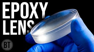
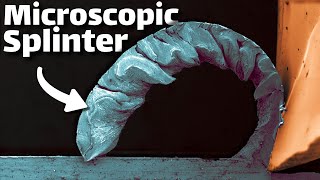
Microlenses are tiny optical devices used to focus light onto cameras and fiber optics. While debugging a different project, I stumbled on a technique that made hemispherical depressions. So I made some microlenses.
CONSIDER SUBSCRIBING 🥰
☕Buy me a coffee? https://www.buymeacoffee.com/Breaking...
🔬Or Patreon if that's your jam: / breakingtaps
📢Twitter: / breakingtaps
💻Discord: / discord
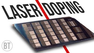
==== Laser Parameters ====
Had some requests for more details about the laser parameters. I'm not sure how much this is dependent on my particular machine vs. generally applicable, but in case it helps:
- 50W fiber laser (non-MOPA). Generic out of china, JPT fiber laser inside
- Power ranged from 2-20%, 40kHz frequency, 500mm/s to 3000mm/s, 63mm f-theta lens, single pass
- Most good ablation craters were in the 10-15% power range. Speed from 1500 to 3000mm/s depending on how much spacing you want between craters.
- Power in range from 6-10% tends to create dimples and spikes. Below 6% and there's no visible effect
- 0.05mm stepover on hatching
- Wafer was 111 orientation thick (500um?) wafer
==== Equipment and techniques ====
- nGauge AFM from ICSPI: https://www.icspicorp.com/
- AFM Scans are post processed in Gwyddion (http://gwyddion.net/) and 3D images rendered in Blender
- Thermo Phenom XL scanning electron microscope
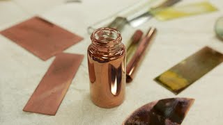
- Metal assisted chemical etching: https://en.wikipedia.org/wiki/Metal_a...
==== Timeline ====
0:00 Intro
0:44 Metal Assisted Chemical Etching
2:25 Strange observation
3:42 Hypothesis #1: heavy oxidation
4:32 Hypothesis #2: Si-Ag "doping"
6:19 Hypothesis #3: indiscriminate etching
7:26 HNA etchant
8:26 Safety Disclaimer
10:22 Etching with HNA
12:16 PDMS molding
14:42 Do they focus light?
16:01 Molding problems
17:47 Other fun phenomena