Published On Dec 24, 2021
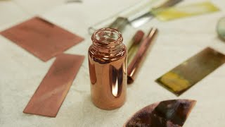
Today we're doping silicon wafers with a phosphoric acid and a fiber laser.
CONSIDER SUBSCRIBING 🥰
☕Buy me a coffee? https://www.buymeacoffee.com/Breaking...
🔬Or Patreon if that's your jam: / breakingtaps
📢Twitter: / breakingtaps
💻Discord: / discord
==== Details ====
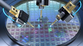
Impurity dopants are traditionally introduced into a wafer via thermal diffusion, or ion implant. There is an alternate method using lasers to drive the dopant into the wafer, a sort of targeted thermal diffusion. This technique is used in the solar panel industry to form back contacts and selective emitters.
The laser selectively vaporizes the phosphoric acid and melts the silicon, allowing phosphorus to diffuse into the molten region. After the laser pulse ends, the silicon resolidifies and the impurity is trapped inside.
Sam's video on RIE: • Etching Silicon with Plasma - Reactiv...
==== Analysis Equipment ====
nGauge AFM from ICSPI (https://www.icspicorp.com/)
Phenom XL SEM from Thermo
Gwyddion for AFM post-processing
Blender for 3D AFM rendering
==== Timeline ====
0:00 Intro
0:39 I have no idea what I'm doing
1:09 Doping silicon
2:21 Thermal diffusion
3:19 Ion implantation
4:36 Laser doping
10:06 Resistivity test
10:40 Hot probe test
12:20 Diode test?
15:57 SEM Archive
17:06 Next steps
17:26 New hat!