Published On Oct 7, 2013
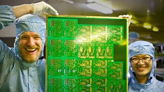
A look at some equipment and wafers used in the manufacture of silicon chip wafers.
200mm and 300mm wafers, die, dice sawing, lead-frame manufacture, automated testing machine (ATE) probing, clean room bunnie suits, photo plots, BGA chip thermal test sockets, and the worlds smallest active FET probes at 100 nanometers for direct wafer probing!
Thanks to Vincent Himpe:
http://www.siliconvalleygarage.com/
Forum: http://www.eevblog.com/forum/blog/eev...
EEVblog Main Web Site:
http://www.eevblog.com
EEVblog Amazon Store:
http://astore.amazon.com/eevblogstore-20
Donations:
http://www.eevblog.com/donations/
Projects:
http://www.eevblog.com/projects/
Electronics Info Wiki:
http://www.eevblog.com/wiki/
show more