Published On Dec 21, 2023
A visit to ASML with a deep dive into diffraction and imaging:
0:00 Intro
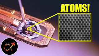
3:14 How big big are chip patterns nowadays?
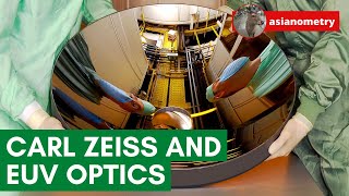
5:00 Arriving at ASML Veldhoven
5:50 Interview Sander Blok part 1
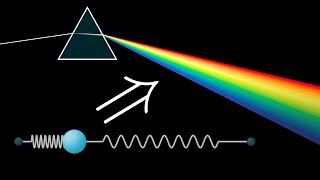
7:40 About diffraction and image formation
9:36 Fraunhofer (far field) interference / diffraction explained
11:15 Diffraction on photolithography masks
15:11 About critical dimension
17:27 Example of computational photolithography
19:23 Interview Sander Blok part 2
21:46 EUV is difficult...
by the way, the frequency of the tin droplets apparently is 50.000 not 15.000 per second.
Animations were made using a Phyton script for Nvidia cuda, which was supplied to me by / @diffractionlimited
The script with instructions to install it can be downloaded from github:
https://github.com/0x23/WaveSimulator2D
Third party images / video:
Sleepy guy: • How To Sleep On Your Desk
Source mask optimization:
https://opg.optica.org/directpdfacces...
If you cannot access the article, search for the title in google: " Source mask optimization using the covariance matrix adaptation evolution strategy"
Royalty free music used:
Road Trip - Slynk
Sharp Edges - half.cool
Floating - Early Birds
All imagery inside the ASML manufacturing facilities is stock video material shown Courtesy of ASML and IBM.
ASML YouTube Channel: / @asmlcompany
Want to work at ASML?: https://www.asml.com/en/careers/find-...
Into viewing wave simulations? Nils Berglund has a ton of them:
• Optics (refraction, diffraction, and ...
Did I forget anyone? Please let me know and we will work it out.