Published On Apr 12, 2022
What a PCB is made of (build-up), determining a suitable build-up, and manufacturer/manufacturing considerations. Second part of video discusses how to choose a suitable stack-up for your PCB design (i.e. what sequence of layers you should assign (GND/PWR/SIG)) for signal integrity, EMI, etc.
[SUPPORT]
Mixed-signal hardware design course: https://phils-lab-shop.fedevel.education
Free trial of Altium Designer: https://www.altium.com/yt/philslab
PCBA from $0 (Free Setup, Free Stencil): https://jlcpcb.com/RHS
Patreon: / phils94
[LINKS]
GitHub: https://github.com/pms67
Rick Hartley Video: • [LIVE] How to Achieve Proper Groundin...
[TIMESTAMPS]
00:00 Intro
00:06 Altium Designer Free Trial
(Build-Up)
00:27 Build-Up Basics
01:58 Layer Count
02:50 Prepreg
03:40 Core
04:18 Copper Foil
05:21 Manufacturability
06:36 Example Manufacturer Build-Up
07:23 Example Controlled Impedance Suggestion
07:49 Altium Designer Layer Stack Manager & Impedance Set-Up
09:13 PCB Manufacturer Build-Up Section
(Stack-Up)
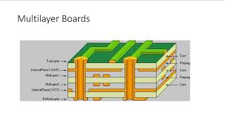
09:56 Stack-Up Basics
10:57 Layer Types
12:09 "Golden Rules" for Determining Stack-Up
13:18 Goal: Prevent Fields from Spreading
13:58 Adjacent PWR + GND Layers
14:34 Improving a 4-Layer Stack-Up
17:05 Return/Transfer Vias
17:49 Additional Stack-Up Tips
18:55 Good Multi-Layer Stack-Ups
19:51 Rick Hartley Video
ID: QIBvbJtYjWuHiTG0uCoK