Published On Dec 5, 2021
Mixed-signal hardware design course: https://phils-lab-shop.fedevel.education
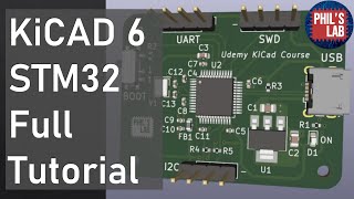
Entire step-by-step PCB design process going through the schematic, layout, and routing of a 'barebones' STM32F4-based PCB including USB, a sensor, GPIO header, and small power supply circuitry in Altium Designer. All the way from schematic creation, through to four-layer PCB layout and routing, as well as sending it off for manufacture and assembly via JLCPCB.
[SUPPORT]
Free trial of Altium Designer: https://www.altium.com/yt/philslab
PCBA from $0 (Free Setup, Free Stencil): https://jlcpcb.com/RHS
Patreon: / phils94
[LINKS]
Git: https://github.com/pms67
KiCad Version: • KiCad STM32 + USB + Buck Converter PC...
Altium Symbol and Footprint Creation: • Symbol and Footprint Creation | Altiu...
[TIMESTAMPS]
00:00 Introduction
01:12 JLCPCB
01:35 Altium Designer Free Trial
01:55 Part Selection
(SCHEMATIC)
05:47 Project Creation, Schematic Creation, Libraries
09:41 STM32 Circuitry (STM32F411)
29:36 Sensor Circuitry (MPU-6050)
40:49 USB and Power Supply Circuitry
52:33 STM32 Pinout with STM32CubeIDE
1:05:31 SWD Circuitry
1:10:23 Annotating Schematic
1:11:30 Cleaning Up Schematic
1:15:03 Electrical Rules Check (ERC)
(PCB)
1:16:17 PCB Creation
1:17:10 Design Rules and Manufacturer Capabilities
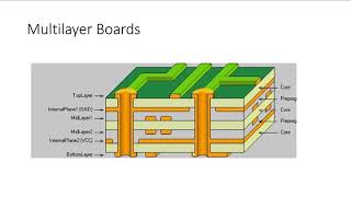
1:20:00 Layer Stackup and Controlled Impedance Traces
1:24:25 Rough Layout and Component Placement
1:25:36 STM32 Layout
1:41:25 Sensor Layout
1:45:05 USB and Power Supply Layout
1:49:25 Mounting Holes
1:51:20 Board Outline
1:53:41 Refining Component Layout
1:55:19 Routing
2:16:39 Internal Layers (Ground Planes)
2:19:20 Ground Vias
2:21:15 Power Routing (+3V3)
2:30:39 Design Rule Check (DRC)
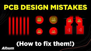
2:33:36 Silkscreen (Text and Logo)
2:35:49 Tooling Holes
(Production)
2:36:40 Gerber Files
2:41:40 Footprint Position (Pick and Place) File
2:42:59 Bill of Materials (BOM) File
2:44:50 Ordering at JLCPCB
ID: QIBvbJtYjWuHiTG0uCoK